平台:vivado2018.3
芯片:xc7a100tfgg484-2 (active)
在FPGA中实现超高位宽加减法器(如256)时,时序收敛常成为瓶颈。由于进位链(Carry Chain)跨越多级逻辑单元,关键路径延迟会随位宽指数增长,导致时钟频率急剧下降。针对这一问题,现在使用如下方式优化大位宽加减法器的时序。
这里使用进位选择加减法器,通过并行计算和进位预测技术,优化加减法器的路径延时,提高整体的运算速度。
优化的核心机制:模块的拆分与并行处理
这里使用减法为例。
1、将输入位宽拆分进行并行处理。
将输入高位宽数据拆分为两部分,低位宽数据和高位宽数据。
使用并行减法器代替高位宽减法器。使用低位减法器(add_lower)计算低位宽数据的差值。同时计算高位宽的减法结果,根据减法器的结构,提前计算借位为0(add_upper0)和借位为1(add_upper1)的两种计算结果。
2、输出结果
根据低位减法器(add_lower)输出借位cout决定高位结果的选取。假如借位为0,选择add_upper0的无借位结果。如果借位为1,选择add_upper1的带借位结果。将最终结果进行拼合。
代码展示
这里都使用vivado的加法器,添加vio和ila的工程。
不使用进位选择。
c_addsub_0 u_c_addsub_0 (.A                                 (dataa                             ), // input wire [255 : 0] A.B                                 (datab                             ), // input wire [255 : 0] B.CLK                               (clock                             ), // input wire CLK.ADD                               (1'b0                              ), // input wire ADD.C_IN                              (1'b1                              ), // input wire C_IN.C_OUT                             (                                  ), // output wire C_OUT.S                                 (result                            )// output wire [255 : 0] S
);
使用进位选择。
// *********************************************************************************/
// Project Name :
// Author       : i_huyi
// Email        : i_huyi@qq.com
// Creat Time   : 2025/4/17 9:30:25
// File Name    : .v
// Module Name  :
// Called By    :
// Abstract     :
//
// CopyRight(c) 2020, xxx xxx xxx Co., Ltd..
// All Rights Reserved
//
// *********************************************************************************/
// Modification History:
// 1. initial
// *********************************************************************************/
// *************************
// MODULE DEFINITION
// *************************
`timescale 1 ns / 1 ps
module add_sub_timing#(
parameter               WIDTH = 256)(
input  wire          [WIDTH-1:0] dataa                , //
input  wire          [WIDTH-1:0] datab                , //
output wire          [WIDTH-1:0] result               , //
input  wire                      clock                  // );
//----------------------------------------------
// localparam
//----------------------------------------------//----------------------------------------------
// register
//----------------------------------------------//----------------------------------------------
// wire
//----------------------------------------------
wire                      lower_cout           ;
wire        [WIDTH/2-1:0] lower_result         ;
wire        [WIDTH/2-1:0] upper0_result        ;
wire        [WIDTH/2-1:0] upper1_result        ;
wire          [WIDTH-1:0] dataa_w              ;
wire          [WIDTH-1:0] datab_w              ;
wire          [WIDTH-1:0] result_w             ;
//----------------------------------------------
// assign
//----------------------------------------------
assign		dataa_w     = dataa                 ;
assign		datab_w     = datab                 ;
assign		result      = result_w              ;
assign      result_w    = {(({WIDTH/2{(~ lower_cout)}} & upper0_result) | ({WIDTH/2{lower_cout}} & upper1_result)),lower_result};
//------------------------------------------------------------
//------------------------------------------------------------
c_addsub_1 add_lower (.A                                 (dataa_w[WIDTH/2-1:0]              ), // input wire [127 : 0] A.B                                 (datab_w[WIDTH/2-1:0]              ), // input wire [127 : 0] B.CLK                               (clock                             ), // input wire CLK.ADD                               (1'b0                              ), // input wire ADD.C_IN                              (1'b1                              ), // input wire C_IN.C_OUT                             (lower_cout                        ), // output wire C_OUT.S                                 (lower_result                      )// output wire [127 : 0] S
);c_addsub_1 add_upper0 (.A                                 (dataa_w[WIDTH-1:WIDTH/2]          ), // input wire [127 : 0] A.B                                 (datab_w[WIDTH-1:WIDTH/2]          ), // input wire [127 : 0] B.CLK                               (clock                             ), // input wire CLK.ADD                               (1'b0                              ), // input wire ADD.C_IN                              (1'b0                              ), // input wire C_IN.C_OUT                             (                                  ), // output wire C_OUT.S                                 (upper0_result                     )// output wire [127 : 0] S
);c_addsub_1 add_upper1 (.A                                 (dataa_w[WIDTH-1:WIDTH/2]          ), // input wire [127 : 0] A.B                                 (datab_w[WIDTH-1:WIDTH/2]          ), // input wire [127 : 0] B.CLK                               (clock                             ), // input wire CLK.ADD                               (1'b0                              ), // input wire ADD.C_IN                              (1'b1                              ), // input wire C_IN.C_OUT                             (                                  ), // output wire C_OUT.S                                 (upper1_result                     )// output wire [127 : 0] S
);//------------------------------------------------------------
//------------------------------------------------------------//------------------------------------------------------------
//------------------------------------------------------------
endmodule
顶层top
// *********************************************************************************/
// Project Name :
// Author       : i_huyi
// Email        : i_huyi@qq.com
// Creat Time   : 2025/2/10 10:20:41
// File Name    : .v
// Module Name  :
// Called By    :
// Abstract     :
//
// CopyRight(c) 2020, xxx xxx xxx Co., Ltd..
// All Rights Reserved
//
// *********************************************************************************/
// Modification History:
// 1. initial
// *********************************************************************************/
// *************************
// MODULE DEFINITION
// *************************
`timescale 1 ns / 1 ps
module top_add_sub#(
parameter               U_DLY = 1'b1)(
input  wire                      clk_p                , //
input  wire                      clk_n                  //);
//----------------------------------------------
// localparam
//----------------------------------------------parameter       WIDTH = 256;
//----------------------------------------------
// register
//----------------------------------------------//----------------------------------------------
// wire
//----------------------------------------------
wire               [WIDTH-1:0] dataa                ; //
wire               [WIDTH-1:0] datab                ; //
wire               [WIDTH-1:0] result                ; // //----------------------------------------------
// assign
//----------------------------------------------
vio_0 u_vio_0 (.clk                               (clock                             ),// input wire cl.probe_out0                        (dataa                             ),  // output wire [255 : 0] probe_out0.probe_out1                        (datab                             )// output wire [255 : 0] probe_out1
);
//------------------------------------------------------------
//------------------------------------------------------------clk_wiz_0 u_clk_wiz_0(// Clock out ports.clk_out1                          (clock                             ),     // output clk_out1// Status and control signals.locked                            (aclr                              ),       // output locked// Clock in ports.clk_in1_p                         (clk_p                             ),    // input clk_in1_p.clk_in1_n                         (clk_n                             ));    // input clk_in1_n
//------------------------------------------------------------
//------------------------------------------------------------//c_addsub_0 u_c_addsub_0 (
//    .A                                 (dataa                             ), // input wire [255 : 0] A
//    .B                                 (datab                             ), // input wire [255 : 0] B
//    .CLK                               (clock                             ), // input wire CLK
//    .ADD                               (1'b0                              ), // input wire ADD
//    .C_IN                              (1'b1                              ), // input wire C_IN
//    .C_OUT                             (                                  ), // output wire C_OUT
//    .S                                 (result                            )// output wire [255 : 0] S
//);add_sub_timing u_add_sub_timing(.dataa                             (dataa                             ), // (input ) .datab                             (datab                             ), // (input ) .result                            (result                            ), // (output) .clock                             (clock                             )// (input ) );//------------------------------------------------------------
//------------------------------------------------------------ila_0 your_instance_name (.clk(clock), // input wire clk.probe0(dataa    ), // input wire [255:0]  probe0  .probe1(datab    ), // input wire [255:0]  probe1 .probe2(result   ) // input wire [255:0]  probe2
);
//------------------------------------------------------------
//------------------------------------------------------------
endmodule
代码仿真。
`timescale 1ns / 1ps
//
// Company:
// Engineer:
//
// Create Date: 2025/03/26 13:54:03
// Design Name:
// Module Name: tb_float_div_nd
// Project Name:
// Target Devices:
// Tool Versions:
// Description:
//
// Dependencies:
//
// Revision:
// Revision 0.01 - File Created
// Additional Comments:
//
//module tb_add_sub;
parameter                 WIDTH = 256          ; reg                       clock                ; //
reg                       rst_n                ; //
reg           [WIDTH-1:0] dataa                ; //
reg           [WIDTH-1:0] datab                ; // wire          [WIDTH-1:0] result               ;
wire          [WIDTH-1:0] result_1             ; wire    flog;
assign  flog = (result == result_1 ) ? 1 : 0;c_addsub_0 u_c_addsub_0 (.A                                 (dataa                             ), // input wire [255 : 0] A.B                                 (datab                             ), // input wire [255 : 0] B.CLK                               (clock                             ), // input wire CLK.ADD                               (1'b0                              ), // input wire ADD.C_IN                              (1'b1                              ), // input wire C_IN.C_OUT                             (                                  ), // output wire C_OUT.S                                 (result                            )// output wire [255 : 0] S
);add_sub_timing u_add_sub_timing(.dataa                             (dataa                             ), // (input ) .datab                             (datab                             ), // (input ) .result                            (result_1                          ), // (output) .clock                             (clock                             )// (input ) );initial
beginclock   = 0;rst_n   = 0;dataa   = 0;datab   = 0;
//        #100;
//        rst_n   =1;
//        #100;
//        dataa   = 'd128;
//        datab   = 'd64;
//
//        #100;
//        dataa   = 'd55;
//        datab   = 'd44;#100;$stop;endalways@(posedge clock)
begindataa   <=   $random & 32'hfff;datab   <=   $random & 32'hfff;
endalways#5 clock = ~clock;endmodule
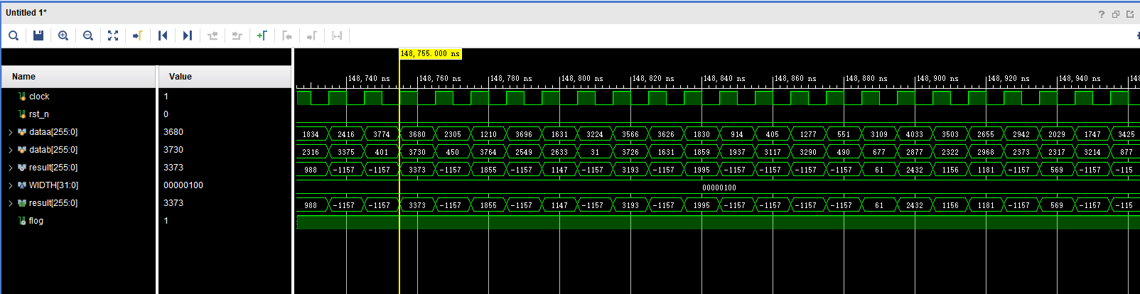
仿真结果
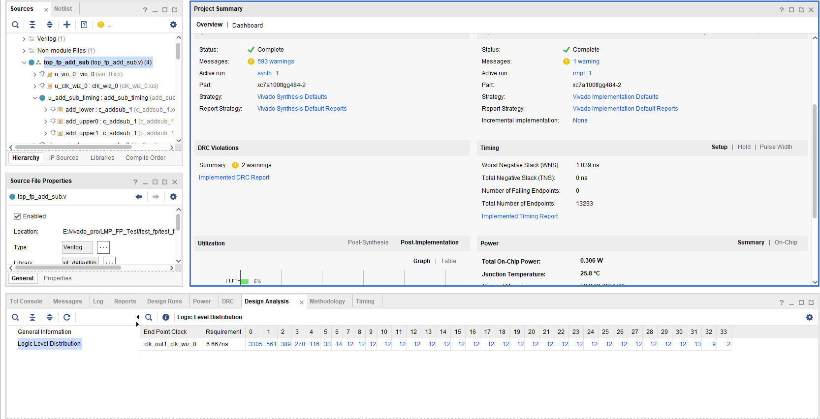
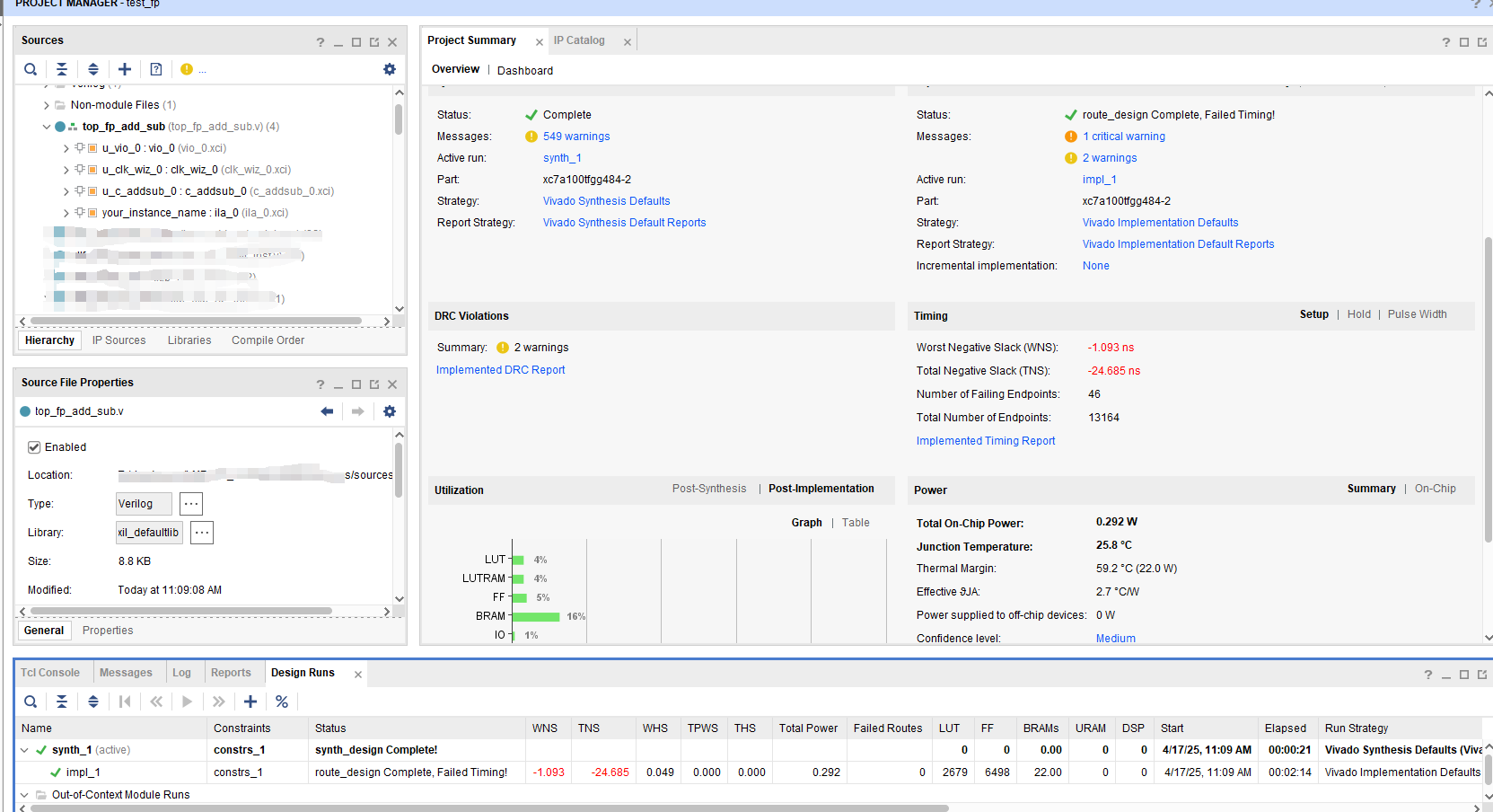
工程综合效果
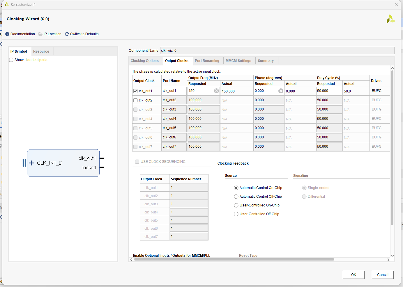
pll输出时钟150MHZ
256位宽加法器设置
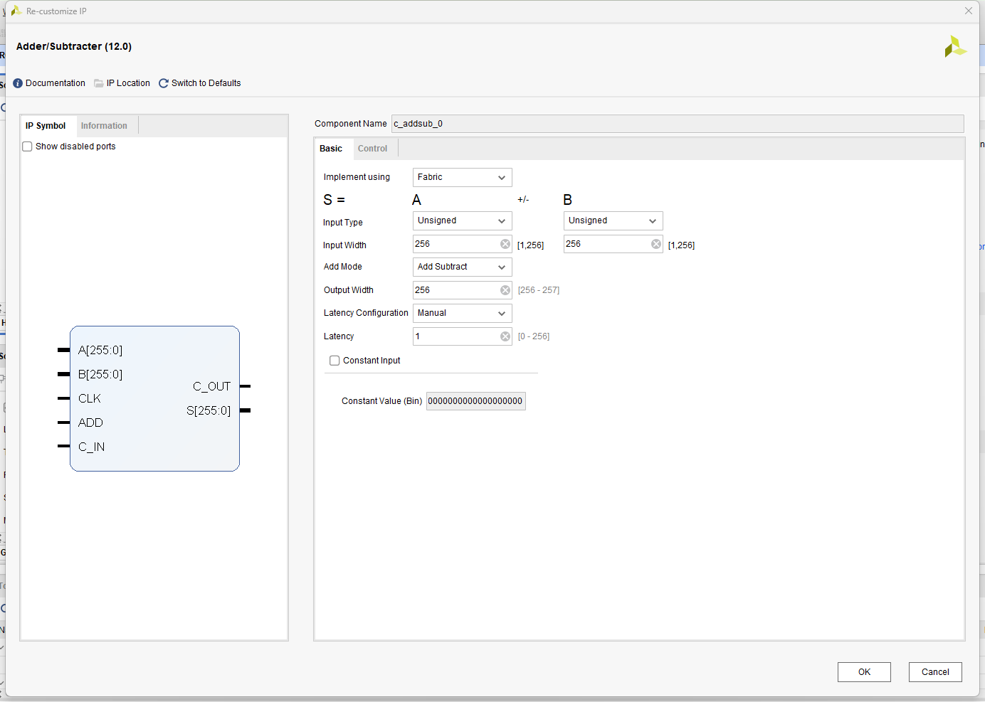
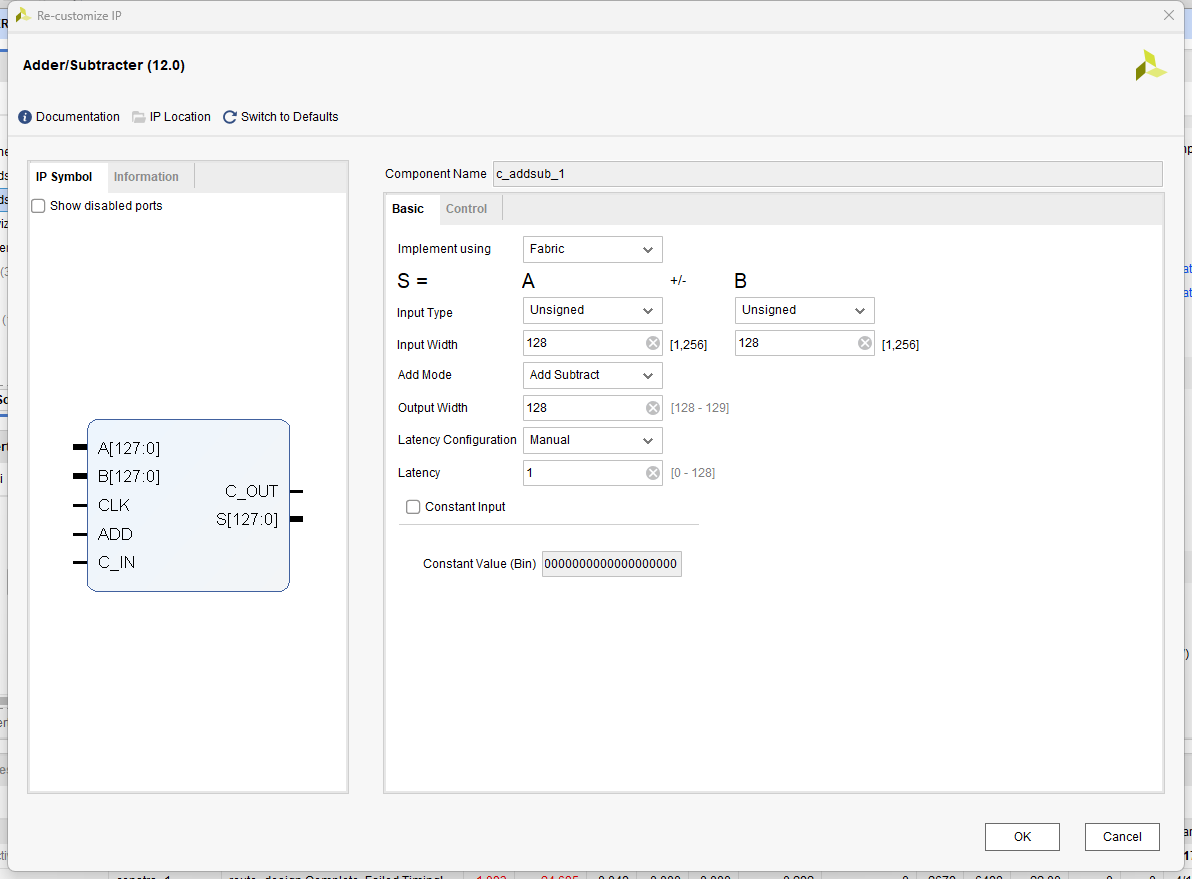
128位宽加法器设置
使用高位宽加减法器
综合时序
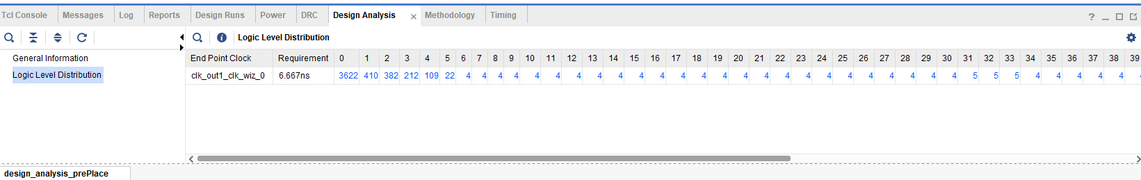
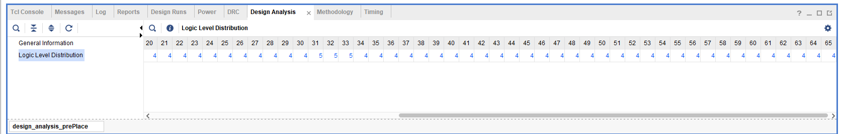
逻辑级数
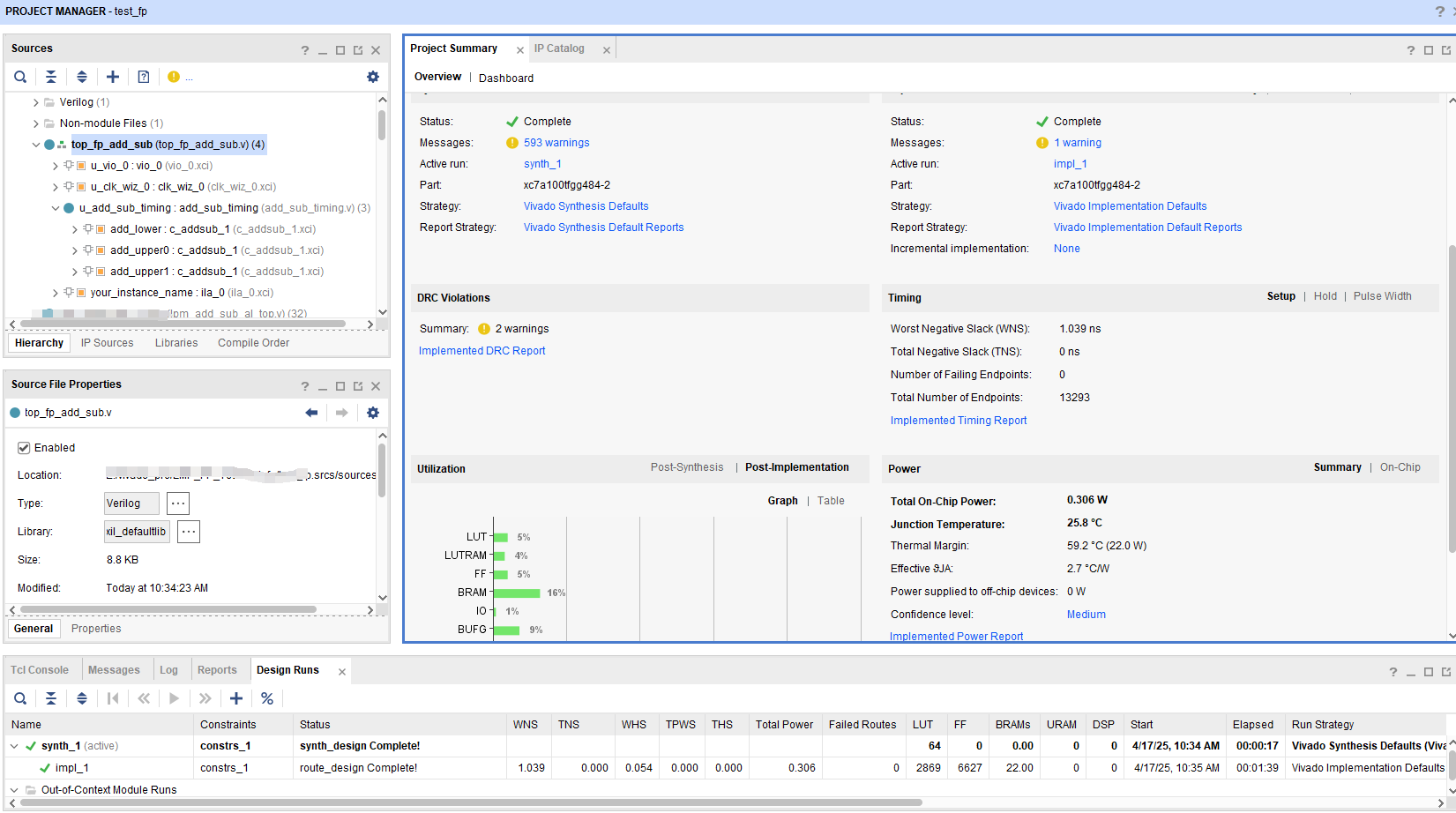
使用进位选择加减法器优化
综合时序
查看逻辑级数